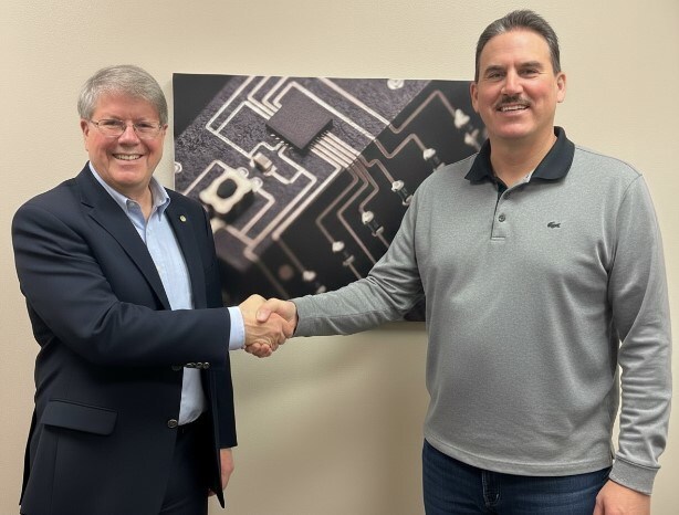
GLS and APES Partner to Advance Semiconductor Packaging and Heterogeneous Integration with New R&D Initiative
Strategic collaboration combines ChipForge™ fabrication and AI-driven additive manufacturing to deliver end-to-end semiconductor design, packaging, and scalable manufacturing solutions.
Image Courtesy: Public Domain
Great Lakes Semiconductor (GLS) and Advanced Printed Electronic Solutions (APES) have entered a strategic partnership to launch a new initiative focused on advanced semiconductor packaging and heterogeneous integration. This collaboration will enable design-to-manufacturing services for rapid, low-through-high volume, and mass customization of GLS-fabricated semiconductor and sensor devices. As part of this initiative, the two companies will establish a joint research and development center that will begin operations at the APES lab in Fishkill, NY, with plans to transition to GLS facilities, where joint manufacturing operations are anticipated.
Integrated Technology and Manufacturing Capabilities
According to Dr. Richard Thurston, CEO of GLS, the partnership leverages both companies' technology portfolios by tightly integrating GLS's proprietary chip fabrication processes with advanced packaging and related electronics, all within a unified manufacturing workflow in each GLS- ChipForge™ unit. This approach aims to address the demand for domestic, cost-effective, end-to-end chip manufacturing.
Key enabling technologies include the GLS modular ChipForge™ semiconductor platform and the GLS proprietary Fab-as-a-Service ("FaaS™) model, and the APES suite of additive manufactured electronics (AME) solutions. Notably, APES's proprietary Matrix6D AME platform—a software-defined, AI-driven swarm factory—will play a central role. By integrating ChipForge™ semiconductors and sensor devices with APES's diverse AME platforms, the collaboration supports a broad spectrum of applications throughout the development lifecycle. This includes early concept design, prototyping, batch production, and large-scale manufacturing of basic die packages, multi-chiplet or sensor integrations, and more. These solutions accommodate various substrates, both rigid and flexible, and are adaptable to numerous shapes and sizes.
Dr. Rich Neill, CEO of APES, explained that the companies will be able to directly embed ChipForge™ -fabricated semiconductors and sensors into rigid or flexible 3D structural substrates, serving applications in autonomous vehicles, medical devices, robotics, electronic assemblies, and a wide range of commercial and defense products.
Implementation Plan and Future Outlook
The collaboration will commence immediately at the APES Fishkill, NY labs, with a planned transition to GLS facilities by the third quarter of 2026. Dr. Neill emphasized that utilizing a range of facilities for research, development, and manufacturing will foster an ideal ecosystem while supporting local economic and workforce development needs.
Dr. Thurston stated that the ultimate objective is to co-locate GLS and APES research and development, design services, chip manufacturing, and back-end package integration under one roof. Once this integrated model is validated, GLS intends to replicate and scale the innovative manufacturing blueprint to additional sites and international partners.